DEUVtek builds precision laser process and metrology systems for advanced packaging and compound semiconductor industries.
Sawing became laser dicing. Grinding is becoming laser thinning. Drilling is becoming DOE-shaped via formation. One closed loop — from beam design through processing to 3D NIR verification — a control depth that neither pure tool vendors nor pure metrology vendors can offer.
“Precision is not a number on a datasheet — it is a discipline built into every optic, every motion, every habit. That discipline is what we brought from Japan to DEUVtek.”
“We aim to be a system-level force in the reorganization of the global semiconductor supply chain — not a single equipment vendor.”
Proprietary metasurface and diffractive optics — command of beam and via geometry above every process.
→Validated process windows for drilling, cutting, and thinning — in glass, SiC, and beyond.
→From optical engine to full tool — in-house integration of laser, motion, and OCT inspection, automation-ready.
→Glass TGV formation, precision cutting, and optical-grade surfaces for the package where photons meet silicon.
Learn more →Laser-formed microchannels in glass and SiC — embedded liquid cooling for AI-era power densities.
Learn more →Damage-free DeepThinning for ultra-thin wafers and stacked dies — breakage <0.01%, sub-30 µm, zero consumables.
Learn more →DOE-embedded glass-based substrate and waveguide assembly for CPO coupling — formed, cut, and 100% OCT-verified on our own line.
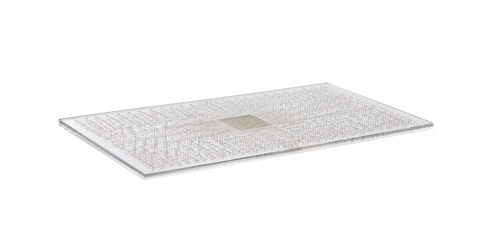
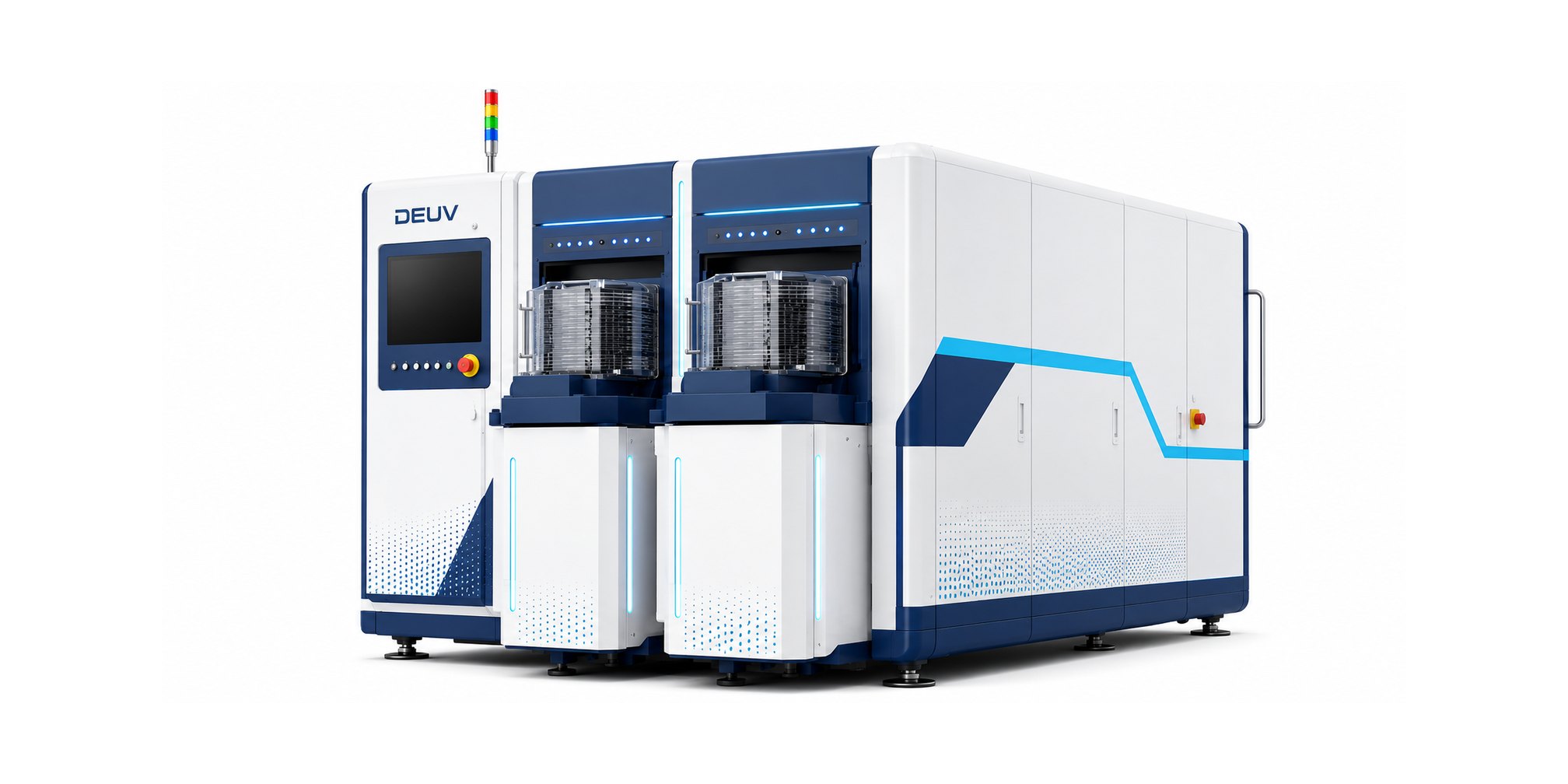
Phalanx-series laser process tools and 3D NIR OCT inspection systems — certification and automation integration included.
Photonic processing replaces energy-hungry mechanical steps — minutes instead of hours, watts instead of consumable-driven kilowatts.
Breakage cut from ~3% to <0.01% — every wafer saved is embodied energy, water, and carbon that never has to be spent twice.
Photonic processing uses no diamond wheels, no slurry, no cleaning chemistry — nothing consumed, nothing sent to waste treatment.
Evaluation lots, foundry quotations, development projects, partnerships — or joining the team. One form, routed to the right people.
DEUVtek Co., Ltd.
Zhongli Lab
1F.-5, No. 192, Zhongyuan Rd., Zhongli Dist., Taoyuan 32063 (Zhongli Industrial Park)
Taipei Office
3F., No. 15, Sec. 1, Nanjing E. Rd., Zhongshan Dist., Taipei 104010
service@deuvtek.com
+886-2-7750-6246